Are you aware that over 90% of cemented carbide inserts, a crucial component in metalcutting, are coated using PVD (Physical Vapor Deposition) techniques? However, this technique also has a growing presence in the medical field, improving the lifespan and performance of medical devices. Understanding and implementing PVD coatings can be a complex task.
With our comprehensive guide, we promise to simplify the world of PVD coating for you – from understanding the basic concepts, to exploring its diverse applications in various industries, and even highlighting the ongoing innovations in the field.
So, if you’re keen to master the art of PVD coating and stay ahead in your industry, let’s dive in and demystify the world of PVD coating together!
1. The Basics of PVD
Physical Vapor Deposition (PVD) is a vacuum process utilized for material transfer from a material source to the substrate, typically used to create nanoparticles and deposit thin layers of material. Various methods are employed in PVD, with recent trends focusing on producing nanostructured, single- and multilayered coatings.
PVD has explored its use in various applications, especially in Electron Beam-Physical Vapor Deposition (EB-PVD) to deposit metallic and ceramic coatings. As a lover of technology, I’m fascinated by the potential that PVD brings to a variety of industries.
2. The History and Evolution of PVD Technology
Physical Vapor Deposition (PVD) is a crucial process in the manufacturing sector, forming an integral part of a multitude of applications. The evolution of this technology has been quite transformative, introducing innovative methodologies while building on the foundation of existing ones.
Initial Developments
The inception of PVD techniques traces back to the advances in vacuum, electronics, magnetism, and plasma technologies, as well as the strides in gaseous chemistry. Cathode sputtering, used for coating fabrication, was one of the early techniques developed as early as the 1930s. Commercial utilization of this method started around the 1950s.
Proliferation of PVD Methods
The technological landscape of PVD experienced considerable expansion and diversification with the advent of multiple techniques, each with distinct characteristics and applications. Evaporation techniques like arcing developed in tandem with sputtering, thus broadening the PVD process spectrum.
As an expert in material science, I am fascinated by the remarkable versatility of PVD techniques in adapting to diverse manufacturing demands.
Modern PVD Techniques and Trends
Today’s sophisticated PVD techniques offer potential in the production of nanostructured, single-, and multilayered coatings. A significant focus of recent PVD trends includes reducing the energy footprint and increasing plasma ionization, thereby optimizing thin film quality. Witnessing the evolution of PVD technology, it’s inspiring to see how far we have come and the limitless possibilities the future holds.
3. Benefits of PVD Coating
Physical Vapor Deposition (PVD) coating presents numerous benefits that enhance the functionality, longevity, and aesthetics of materials. Here we are going to delve into the key advantages it offers.
Improved Hardness and Durability
PVD coatings are synonymous with high hardness and wear resistance. According to a study in Science Direct, coatings are commonly used in machining tools due to their high hardness and wear resistance, but can also be applied for jewellery and decorative purposes.
PVD coating increases the lifespan of machining tools by enhancing their durability, reducing friction, and improving thermal properties. This quality renders PVD coating highly desirable in demanding applications like cutting tools for metalworking.
Increased Corrosion and Oxidation Resistance
By depositing a thin, hard layer on the surface of substrates, PVD coatings offer exceptional resistance to corrosion and oxidation. I can’t stress enough the value of these PVD coatings; they’re like protective knights shielding our surfaces from corrosion’s fiery breath. This protective feature finds significant application in environments prone to corrosive substances or high oxidative conditions.
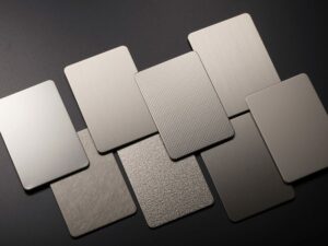
Decorative and Functional Aspects
Apart from their mechanical advantages, PVD coatings serve decorative purposes and are employed in the jewelry industry. Moreover, they provide optical enhancement and aesthetic upgrading, thus widening the scope of their applications. In my years of observing and utilizing PVD techniques, I have come to appreciate the significant improvements they bring in material properties.
4. PVD Coating Technologies
Physical Vapor Deposition (PVD) coating technologies involve diverse techniques that transform material phases for deposition onto a substrate. Each technology carries distinct characteristics and applications, allowing for precise customization of coating properties.
Sputter Deposition
Sputter deposition is a PVD process wherein high-energy ions bombard a target material, causing atoms to sputter off and deposit onto a substrate. This method offers excellent control over the thickness and composition of the deposited layer.
The extent of control we can exercise over the coating properties, especially with sputter deposition, never ceases to amaze me. It is widely used in applications such as semiconductors and optical coatings.
Evaporative Deposition
Evaporative deposition involves heating a source material until it evaporates and subsequently deposits on a substrate. It’s a straightforward, cost-effective method used for creating thin films in microelectronics and optical applications. However, it lacks control over the deposited layer thickness that sputter deposition offers.
Arc Evaporation
Arc evaporation uses an electric arc to vaporize the source material, resulting in a plasma cloud which condenses onto the substrate. It produces coatings with high density and excellent adhesion. Some examples of its application include hard coatings for wear resistance, decorative coatings, and coatings for enhanced conductivity.
Laser Ablation
Laser ablation employs laser pulses to vaporize the target material, which then condenses onto a substrate. It allows for precise control over the deposition process and is typically used for special applications such as fabricating superconductors and high-temperature material. I always find laser ablation fascinating; the precision and control it offers feels like a futuristic art form to me.
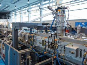
5. The PVD Coating Process
The Physical Vapor Deposition (PVD) Coating Process is a vacuum-based method that is used to produce thin films and coatings on various substrates, including metals, ceramics, glass, and polymers. This intricate process involves the transition of material from a condensed phase to a vapor phase, and then back to a thin film condensed phase. Below are the following steps:
Step#1 Pre-Coating
The first stage of the PVD coating process involves pre-coating, which requires meticulous surface preparation and cleaning. This is crucial to ensure that the subsequent coating adheres properly to the substrate.
Surface Preparation Cleaning
Surface preparation and cleaning typically entail the removal of any contaminants on the substrate surface, such as dirt, oils, or oxidation layers. This process is necessary to provide a clean and optimal surface for the PVD coating to adhere to, and it involves the following:
- Surface condition assessment: This step entails evaluating the condition of the surface before commencing the preparation process. According to TWI-Global, there are standards that can assist with this assessment, such as with BS EN ISO 8501-1, which provides details of rust grades ranging from A-D for steel surfaces.
- Roughening: The process of roughening the surface helps improve adhesion of the coating by increasing the surface area and creating mechanical interlocking sites.
- Dry abrasive grit blasting: This technique is used to clean the surface and provide a rough profile to enhance adhesion.
- Machining and macro roughening processes: These are used to further increase the surface area and roughness, aiding in better adherence to the coating material.
Cleaning
Cleaning, another crucial aspect of precoating, includes the following activities:
- Gross cleaning: This involves removing large amounts of contaminants often by eliminating some of the substrate surface.
- Specific cleaning: This process is targeted towards removing a specific contaminant such as particulates, or hydrocarbons. From my experience, consistent and accurate specific cleaning is an art in itself, a delicate dance of balance.
- Solvent cleaning (SSPC-Surface Preparation (SP)-1): This cleaning method entails the use of solvents to remove contaminants like oil, grease, dirt, soil, salts, and films.
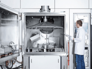
Step#2 The Coating Process
The coating process, specifically Physical Vapor Deposition (PVD), is an environmentally friendly method to deposit thin layers of material using atomic transfer under vacuum conditions, often used for the production of nanomaterials and industrial applications. This process is broadly divided into two crucial steps:
Evaporation
Evaporation is a common method of thin-film deposition, where the source material is heated and evaporated in a vacuum environment. This ensures a clean and controlled environment for the process, allowing vapor particles to travel directly to the target object. Here are three important aspects to remember in this step:
- High temperature requirement: The source material needs to be heated to high temperatures to evaporate. The heat source may vary depending on the material and the specific technique used.
- Vacuum environment: Evaporation takes place in a vacuum to minimize the interference from other gases, allowing vapor particles to travel directly to the target substrate.
- Source material: The source material starts out in solid form and needs to be carefully selected to ensure it can be successfully evaporated and that the resulting vapors will produce the desired end product when deposited.
Deposition
Deposition occurs when the evaporated particles condense back to a solid state on the target object or substrate. This step requires careful control to ensure uniform coating and proper film properties. Here are three important aspects to remember in this step:
- Controlled environment: The conditions under which deposition occurs, including temperature and vacuum level, must be carefully controlled to ensure uniformity and quality of the deposited film.
- Particle speed: The speed at which the evaporated particles travel and hit the substrate can affect the quality and characteristics of the deposited film.
- Substrate preparation: The target substrate must be properly prepared to accept the deposition, which may include cleaning, surface treatment, or heating, to ensure good adhesion and quality of the coating. Having been through this process numerous times, no detail can be overlooked in substrate preparation-it’s truly the foundation of a successful coating application.
Step#3 Post-Coating
Post-coating refers to the period following the application of a protective or decorative layer on a material, often metal. This crucial phase entails various processes such as curing, drying, and subsequent inspections. Below are the significant topics in this step that should be taken into account:
Quality Inspection and Control
Quality inspection is a systematic exercise performed after the coating process to identify any flaws or deviations from the set standards. Quality control, on the other hand, is a proactive and continuous approach to ensure that the coating process consistently delivers high-quality results by implementing defined standards and practices. Here are three types of quality inspection:
- Thickness measurement: This inspection uses specialized tools such as a paint thickness gauge to measure the thickness of the coating. The thickness of a coating can impact its performance, durability, and appearance, making it an essential aspect of quality control.
- Adhesion testing: This process evaluates the strength of the bond between the coating and the substrate. It is performed using various methods, such as pull-off or cross-cut tests, to ensure the coating’s long-term durability and resistance to peeling or flaking.
- Visual inspection: This is a basic yet critical inspection that involves examining the coated surface for any visible defects or inconsistencies such as runs, sags, or bubbles. This is often the first step in quality inspection as it can easily detect gross errors in the coating application.
6. PVD vs. Other Coating Techniques
Physical vapor deposition (PVD) is a versatile vacuum deposition method used to produce thin films and coatings on a range of substrates. It offers a host of benefits including improved wear resistance, reduced friction, and enhanced corrosion protection. Below is the thorough presentation of the differences in each technique.
PVD vs. CVD
Physical Vapor Deposition (PVD) and Chemical Vapor Deposition (CVD) are both integral techniques in the world of coatings, each having its own unique approach to achieving desired results. PVD operates by evaporating or atomizing depositing species from a solid source, while CVD introduces the depositing species in a gaseous or vapor form. Below is a more vague comparison between the two:
| Criteria |
PVD |
CVD |
| Process |
Vaporization of material from a solid source |
Precursors are introduced in a gaseous form |
| Temperature |
Generally, a high-temperature process, but some methods like DLC coatings work at ~150–200°C |
Typically operates at high temperatures |
| Versatility |
Can deposit a wide range of materials |
Better suited for specific materials |
| Substrate Compatibility |
Can coat a variety of substrates |
May be limited depending on the precursor gases |
As a professional in this industry, I truly appreciate the adaptability and range of applications that PVD offers. Its capacity to produce durable films on a variety of substrates sets it apart from other coating techniques.
PVD vs. Electroplating
PVD employs a high-tech process that vaporizes and condenses metals to be transferred from their original solid state, whereas electroplating involves the immersion of the tool in a liquid solution connected to a power supply, causing the desired coating material to adhere to the tool surface. Below is a more vague comparison between the two:
| Criteria |
PVD |
Electroplating |
| Process |
High-energy vacuum process |
Electrochemical process |
| Environmental Impact |
Lower environmental impact |
Potentially hazardous chemicals can be used |
| Coating Uniformity |
Uniform thin films |
Thickness can vary, often thicker deposits |
| Substrate Compatibility |
Broad range of substrates |
Mainly conductive substrates |
Take note that even if electroplating can provide thick, sturdy coatings, environmental hazards associated with the process can be a major drawback. PVD, on the other hand, offers a more environmentally friendly alternative. Suproto, take pride in our commitment to providing greener solutions in surface coating technology.
PVD vs. Thermal Spraying
PVD utilizes vacuum deposition processes resulting in typically thinner coatings. On the other hand, thermal spraying, while not covered extensively in the provided references, is a popular coating technique that involves the ejection of small molten or semi-molten droplets onto a surface to create a coating, usually resulting in thicker but potentially less uniform coatings. Below is a more vague comparison between the two:
| Criteria |
PVD |
Thermal Spraying |
| Process |
Vacuum-based process |
Coating material is heated and sprayed onto the substrate |
| Temperature |
Typically high-temperature, but low-temperature methods exist |
High-temperature process |
| Coating Thickness |
Thin films |
Thick coatings |
| Substrate Compatibility |
Can coat a variety of substrates |
Can be limited due to high-temperature process |
I am still amused by the way that PVD could provide a better solution for substrates that can’t withstand the high temperatures of thermal spraying.
7. PVD Coating in Industries
Physical Vapor Deposition (PVD) is an advanced coating technique that transforms material on an atomic level into a vapor that is then deposited onto various substrates. This innovative process is carried out in vacuum conditions, resulting in thin films of exceptional purity and high performance.
PVD’s advantageous properties have led to the wide adoption of PVD coatings across multiple industries, providing a multitude of functional benefits. With that, here are the industries where PVD became top-notch:
Automotive Industries
In the automotive industry, PVD coatings are extensively employed to enhance the durability, appearance, and performance of various components. For example, these coatings improve wear resistance in engine parts, increasing the lifespan of vehicles. Furthermore, PVD-coated decorative trim parts offer superior corrosion and scratch resistance.
Aerospace
In the aerospace sector,PVD coatings could significantly enhance the longevity of aerospace components, providing a cost-effective solution for this high-stakes industry. They improve wear and corrosion resistance, especially in turbine engines, leading to improved fuel efficiency and safety. With Suproto’s high-quality PVD coatings promised to help to revolutionize the aerospace industry.
Medical Devices
PVD coatings play an essential role in the medical device industry by providing bio-compatible and anti-corrosive surfaces. PVD coatings could significantly reduce bacterial adhesion to medical implants, leading to decreased infection rates. And the best part is that it improves device lifespan and reduces patient complications.
Microelectronics
Microelectronics extensively leverage PVD for depositing thin films on semiconductor devices. These coatings enhance device efficiency and longevity. As someone with a deep appreciation for technology, I am particularly fascinated by the role of PVD in microelectronics. This industry is constantly evolving, and it is remarkable how a process like PVD can significantly impact device efficiency and longevity.
Dive Deeper Into Our Resources
Looking for more diverse service options? Browse through our handpicked selections:
For some insightful reads, we’ve curated a list of recommended articles just for you:
Still haven’t found what you’re looking for? Don’t hesitate to contact us. We’re available around the clock to assist you.
Conclusion
All throughout this guide on PVD Coating, it’s clear that innovative technology significantly contributes to enhancing products. In my own journey exploring this topic, I’ve grown to appreciate the intricate balance between science, technology, and art that PVD Coating embodies.
So, don’t let your curiosity stop here. Feel free to contact us with any questions or for more in-depth information about our product line. We’re eager to share the marvels of PVD coating with you and help you find the perfect solution for your specific needs.